This revolutionary advancement in 2D material transfer, brought to you by the UoM 2D Courier team, promises to reshape the landscape of electronic device commercialisation.
The research behind this invention has been published in the journal Nature Electronics. See below for a brief summary:
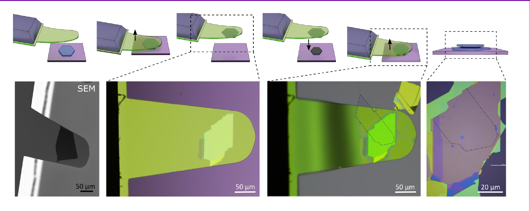
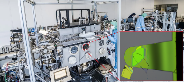
Researchers at the University of Manchester, led by Professor Roman Gorbachev from the National Graphene Institute, have achieved a breakthrough in the transfer of 2D crystals. This pioneering technique, detailed in a recent Nature Electronics publication, utilises a fully inorganic stamp to meticulously ‘pick and place’ 2D crystals into van der Waals heterostructures of up to 8 individual layers within an ultra-high vacuum environment.
Scientists at the University of Manchester Unveil Inorganic Stamp Technology for Creating Atomically Clean Interfaces
Key Achievements:
- Atomically Clean Interfaces: The novel stamp design facilitates the creation of atomically clean interfaces between stacked 2D materials over extended areas, surpassing existing techniques.
- Reduced Strain Inhomogeneity: The rigidity of their innovative stamp design substantially reduces strain inhomogeneity in assembled stacks, showcasing a remarkable improvement in performance.
- Scalability: The demonstrated clean transfer of mm-scale areas of 2D materials opens avenues for their utilisation in next-generation electronic devices, marking a leap forward in scalability.
Professor Roman Gorbachev, lead author comments:
“This ubiquitous transfer-induced contamination, along with the variable strain introduced during the transfer process, has been the primary obstacle hindering the development of industrially viable electronic components based on 2D materials”

Prof. Roman Gorbachev
Advancements and Implications:
- Atomically Clean Interfaces: The use of an inorganic stamp ensures atomically clean interfaces over extended areas, a crucial step towards commercialising 2D material-based electronic devices.
- Strain Minimisation: The new stamp design effectively minimises strain inhomogeneity in assembled stacks, leading to a significant decrease in local variation, particularly at ‘twisted’ interfaces.
- Potential for Designer Crystals: Precise stacking of individual 2D materials holds the potential to engineer designer crystals at the atomic level, unlocking novel hybrid properties.
Overcoming Transfer Challenges:
The breakthrough technique addresses the challenges posed by conventional methods relying on organic polymer membranes or stamps, which introduce surface contamination during the transition from original substrates to target ones.
Stamping Flakes into Stacks
Future Collaboration and Impact:
The University of Manchester has filed a pending patent application to protect both the method and apparatus involved. We are eager to collaborate with industry partners for the wafer-scale transfer of 2D films from growth substrates.
Equipment manufacturers, semiconductor foundries, and electronic device manufacturers with 2D materials in their product roadmap should contact Gareth Jones for any queries.