A vacuum-compatible, dry, adhesive-free process for pristine bonding & de-bonding of atomically thin films
2D materials, such as graphene and transition metal dichalcogenides (TMDs), are key technologies for the semiconductor industry to continue the exponential progress originally charted by Moore’s Law.
Foundries for advanced logic chips are working to integrate TMDs in advanced process nodes to shrink the thickness of transistor channels below the dimensions where electrical transport in silicon and III-V semiconductors breaks down [1]. Additionally, due to its broadband absorption and high charge carrier mobility, graphene is likely to be integrated into optical modulators for the next generation of high-speed data communication systems and photonic circuits. [2]
National Graphene Institute, where 2D Courier was created.
Market focus & product summary:
The growth temperatures required to synthesise high quality, crystalline 2D materials are too high to grow films in-situ on integrated circuits. Instead, 2D material films are grown by chemical vapour deposition (CVD) on ancillary substrates (metal catalysts or inorganic wafers) and must then be transferred onto target substrates via wafer bonding.
Semiconductor bonding equipment is essential for these and many other process flows. Annual sales of bonding equipment are projected to reach $920 million by 2028 (12% CAGR) [3]. Innovations are required for these systems to process atomically thin films in compliance with extremely high throughput and quality standards.
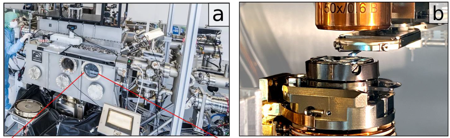
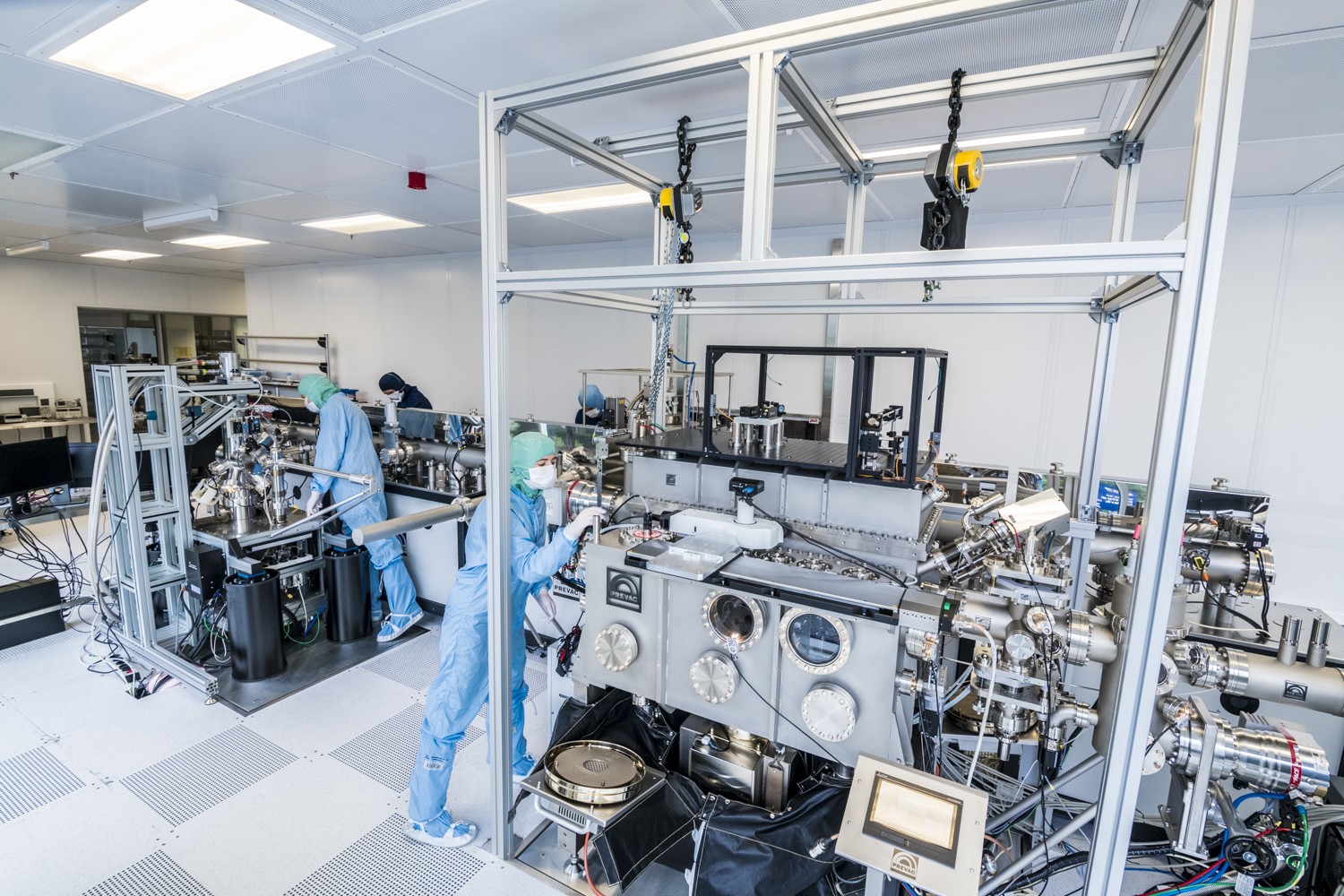
Figures a) and b) show the prototype system working inside an ultra-high vacuum system, which keeps samples extremely clean and avoids contamination from humidity or oxygen.
Value proposition / competitive advantage:
2D Courier is a novel method and apparatus for the pristine transfer of atomically thin films between substrates. It offers the following advantages for the prototyping and mass-manufacture of 2D material devices:
1. Excellent material quality – no contamination from wet etchants or polymer adhesives. The process is fully compatible with vacuum environments and creates atomically pristine heterostructure interfaces.
2. Efficient process flow–a simple pick and place method with no etching or film deposition steps. 2D-Courier bonding apparatus is re-usable and can sequentially stack films into heterostructures.
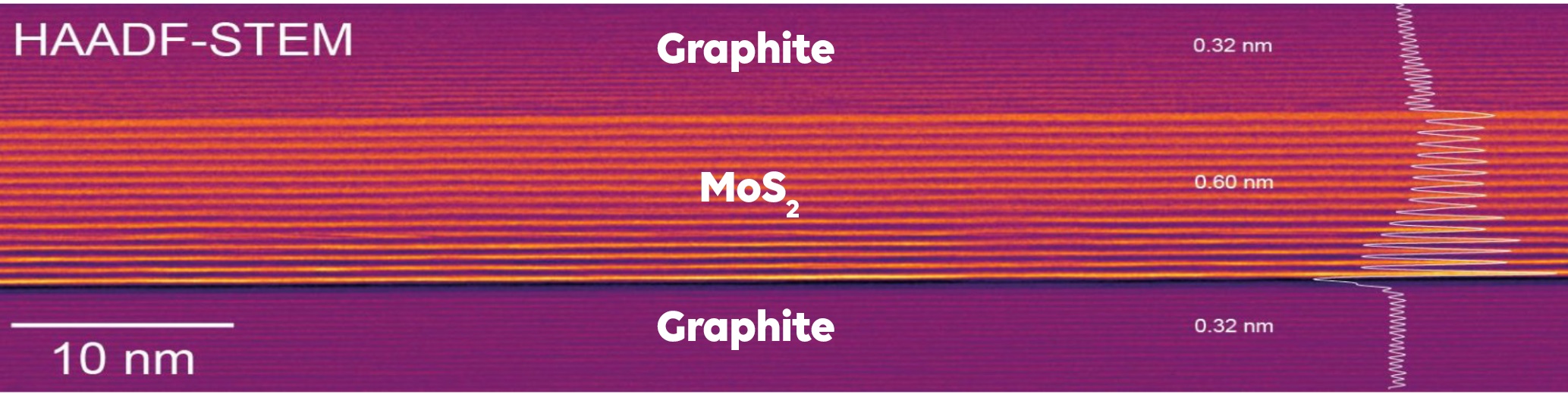
An example of an atomically pristine heterostructure stack.
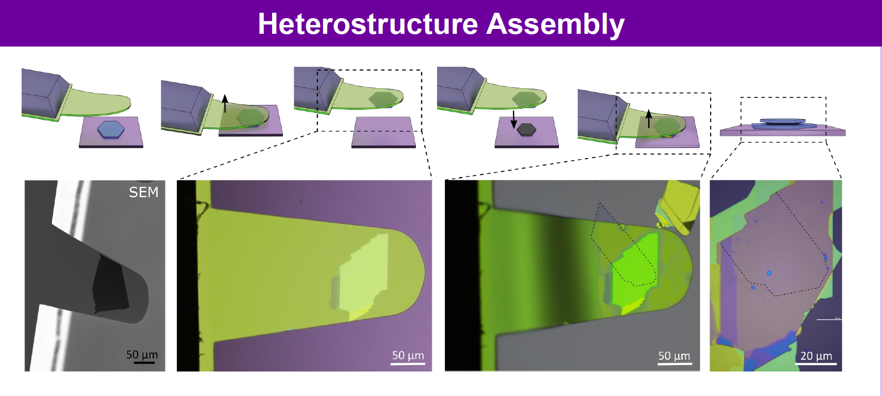
A schematic of the transfer process with images of 2D material films at each step of processing.
2D Courier was created by Prof. Roman Gorbachev’s Condensed Matter Physics Group at The National Graphene Institute. The team have demonstrated transfer of mechanically exfoliated flakes of graphene and TMDs as well as CVD-grown WS2 from SiO2 substrates at mm2 scales.

Prof. Roman Gorbachev
What now?
The University of Manchester team would like to work with industry partners to evaluate the efficacy of this method for wafer- scale transfer of 2D films from CVD growth substrates. They would welcome expressions of interest from:
- Companies using 2D materials in microelectronics products.
- Wafer bonding and MOCVD equipment manufacturers.
- Specialist 2D materials foundries and mainstream semiconductor foundries.
Please get in touch with the Project Manager for more information.
This project has received funding from the European Research Council (ERC) under the European Union’s Horizon 2020 research and innovation programme (grant agreements No 715502 and 649953) and the Royal Society (URF\R\191028). These funding organisations are not responsible for any use that may be made of the information this article contains.
References: [1] IEDM 2023 (Semiwiki); IMEC roadmap; [2] Black Semiconductor; CamGraPhIC; METROGRAPH; [3] Mordor Intelligence
